
Physics - Semiconductors Question with Solution | TestHub
PhysicsSemiconductorsPN junctionHard2 minPYQ_2022
PhysicsHardsingle choice
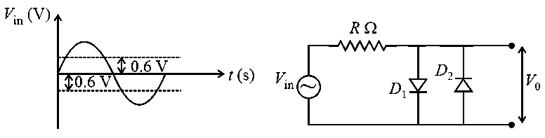
In the given circuit the input voltage is shown in figure. The cut-in voltage of junction diode ( or ) is . Which of the following output voltage waveform across the diode is correct?
Options:
Answer:
D
Solution:
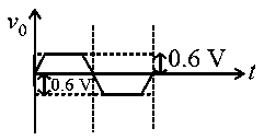
During the positive half cycle of the input waveform, diode is forward biased and diode is reverse biased. Here appears across the output as the diode is conducting. During negative half cycle the diode is reverse biased and is forward biased, so, appears across the output as the diode is conducting in negative direction. This circuit can be used as a voltage limiter. This circuit will not allow any voltage above and below .
Hence, the output waveform is
Stream:JEESubject:PhysicsTopic:SemiconductorsSubtopic:PN junction
⏱ 2mℹ️ Source: PYQ_2022
Doubts & Discussion
Loading discussions...